 | ÐлекÑÑоннÑй компоненÑ: LTC3701 | СкаÑаÑÑ:  PDF PDF  ZIP ZIP |
Äîêóìåíòàöèÿ è îïèñàíèÿ www.docs.chipfind.ru
1
LTC3701
3701fa
APPLICATIO S
U
FEATURES
DESCRIPTIO
U
TYPICAL APPLICATIO
U
2-Phase, Low Input Voltage,
Dual Step-Down DC/DC Controller
The LTC
®
3701 is a 2-phase dual constant frequency cur-
rent mode step-down DC/DC controller providing excellent
load and line regulation. Power loss and noise due to ESR
of the input capacitor are minimized by operating the two
controller output stages out-of-phase.
The LTC3701 provides a 0.8V
±
2% voltage reference and
consumes only 460
µ
A of quiescent current. To further
maximize the life of a battery source, the external
P-channel MOSFET is turned on continuously in dropout
(100% duty cycle).
Switching frequency is internally set at 550kHz, allowing
the use of small inductors and capacitors. For noise sen-
sitive applications, the LTC3701 can be externally syn-
chronized using its phase-locked loop. The frequency can
also be externally set from 300kHz to 750kHz by applying
a voltage to the PLLLPF pin. Burst Mode operation is inhib-
ited during synchronization or when the EXTCLK/MODE
pin is pulled low to reduce noise and RF interference.
The LTC3701 contains independent internal soft-start
circuitry for each controller. Other features include a
power good output voltage monitor and output overvolt-
age and short-circuit protection.
The LTC3701 is available in a small footprint 16-lead nar-
row SSOP package.
s
Out-of-Phase Controllers Reduce Required
Input Capacitance
s
True PLL for Frequency Locking or Frequency
Adjustment
s
Operating Frequency Range: 300kHz to 750kHz
s
Wide V
IN
Range: 2.5V to 10V
s
Constant Frequency Current Mode Architecture
s
Low Dropout: 100% Duty Cycle
s
Power Good Output Voltage Monitor
s
Internal Soft-Start Circuitry
s
Selectable Burst Mode
®
/Pulse Skipping Operation
at Light Loads
s
Output Overvoltage Protection
s
Low Quiescent
Current: 460
µ
A
s
0.8V
±
2% Voltage Reference
s
Small 16-Lead Narrow SSOP Package
s
One or Two Lithium-Ion Powered Applications
s
Notebook and Handheld Computers
s
Personal Digital Assistants
s
Portable Instruments
s
Distributed DC Power Systems
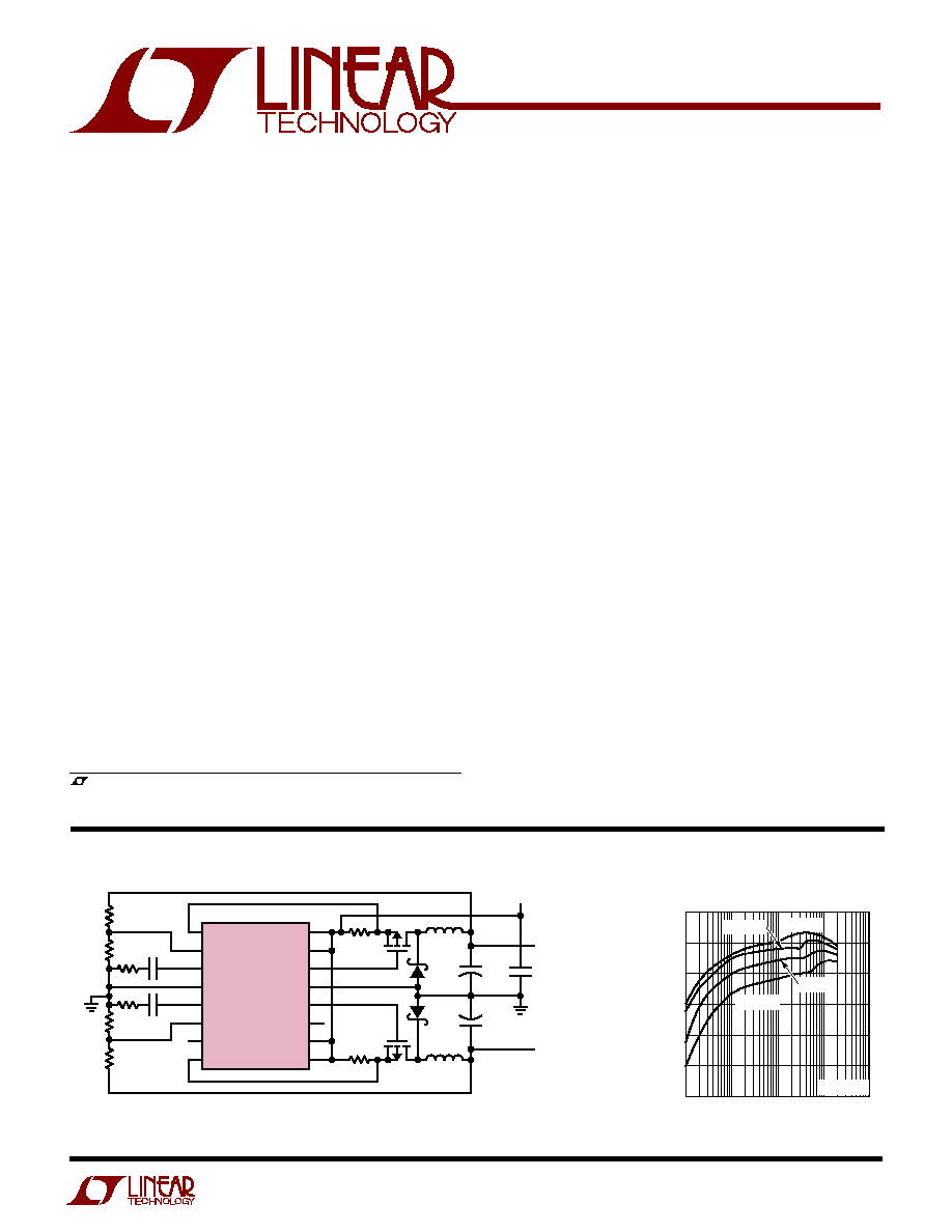
Figure 1. High Efficiency 2-Phase 550kHz Dual Step-Down Converter
Efficiency vs Load Current
+
+
SENSE1
V
FB1
I
TH
/RUN1
SGND
I
TH
/RUN2
V
FB2
PLLLPF
SENSE2
SENSE1
+
V
IN
PGATE1
PGND
PGATE2
PGOOD
EXTCLK/MODE
SENSE2
+
1
3
2
4
6
5
7
8
16
15
14
13
12
11
10
9
LTC3701
220pF
220pF
10k
10k
D1, D2: IR10BQ015 L1, L2: LQN6C-4R7 M1, M2: FDC638P
78.7k
80.6k
100k
169k
L1
4.7
µ
H
47
µ
F
10
µ
F
47
µ
F
0.03
0.03
L2
4.7
µ
H
D1
M1
M2
D2
3701 F01a
V
OUT1
2.5V
2A
V
IN
2.5V TO 9.8V
V
OUT2
1.8V
2A
, LTC and LT are registered trademarks of Linear Technology Corporation.
Burst Mode is a registered trademark of Linear Technology Corporation.
LOAD CURRENT (mA)
60
EFFICIENCY (%)
80
100
50
70
90
1
100
1000
10000
3701 F01b
40
10
V
IN
= 3.3V
V
IN
= 8.4V
V
OUT
= 2.5V
V
IN
= 4.2V
V
IN
= 6V
2
LTC3701
3701fa
(Note 1)
Input Supply Voltage (V
IN
)........................ 0.3V to 10V
SENSE1
, SENSE2
, PGATE1, PGATE2,
PLLLPF, SENSE1
+
, SENSE2
+
,
EXTCLK/MODE Voltages .............. 0.3V to (V
IN
+ 0.3V)
V
FB1
, V
FB2
, I
TH
/RUN1,
I
TH
/RUN2 Voltages .................................. 0.3V to 2.4V
PGOOD Voltage ........................................ 0.3V to 10V
PGATE1, PGATE2 Peak Output Current (<10
µ
s) ....... 1A
Operating Ambient Temperature Range
(Note 2) ...................................................40
°
C to 85
°
C
Storage Ambient Temperature Range ... 65
°
C to 150
°
C
Junction Temperature (Note 3) ............................ 125
°
C
Lead Temperature (Soldering, 10 sec).................. 300
°
C
The
q
denotes specifications which apply over the full operating
temperature range, otherwise specifications are T
A
= 25
°
C. V
IN
= 4.2V unless otherwise noted.
ABSOLUTE AXI U RATI GS
W
W
W
U
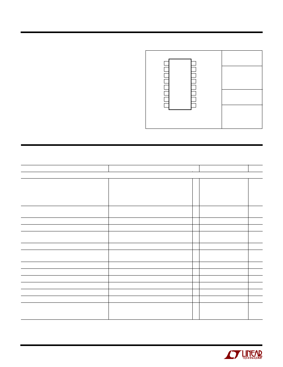
PACKAGE/ORDER I FOR ATIO
U
U
W
ORDER PART
NUMBER
LTC3701EGN
ELECTRICAL CHARACTERISTICS
T
JMAX
= 150
°
C,
JA
= 140
°
C/W
GN PACKAGE
16-LEAD PLASTIC SSOP
1
2
3
4
5
6
7
8
TOP VIEW
16
15
14
13
12
11
10
9
SENSE1
I
TH
/RUN1
V
FB1
SGND
V
FB2
I
TH
/RUN2
PLLLPF
SENSE2
SENSE1
+
V
IN
PGATE1
PGND
PGATE2
PGOOD
EXTCLK/MODE
SENSE2
+
PARAMETER
CONDITIONS
MIN
TYP
MAX
UNITS
Main Control Loops
Input DC Supply Current
(Note 4)
Normal Operation
2.5V < V
IN
< 9.8V
460
780
µ
A
Sleep Mode
2.5V < V
IN
< 9.8V
305
470
µ
A
Shutdown
2.5V < V
IN
< 9.8V, I
TH
/RUN1 = I
TH
/RUN2 = 0V
9
28
µ
A
UVLO
V
IN
< UVLO Threshold
18
30
µ
A
Undervoltage Lockout Threshold
V
IN
Falling
q
1.55
2.00
2.50
V
V
IN
Rising
1.70
2.12
2.55
V
Shutdown Threshold at I
TH
/RUN1, 2
0.2
0.35
0.5
V
Start-Up Current Source on I
TH
/RUN1, 2
V
ITH
/RUN1, 2 = 0V
0.25
0.5
0.85
µ
A
Regulated Feedback Voltage
0
°
C to 70
°
C (Note 5), I
TH
/RUN = 1.3V
q
0.784
0.8
0.816
V
40
°
C to 85
°
C (Note 5)
q
0.774
0.8
0.826
V
Output Voltage Line Regulation
2.5V < V
IN
< 9.8V (Note 5)
0.05
0.20
mV/V
Output Voltage Load Regulation
I
TH
/RUN = 0.9V (Note 5)
0.2
0.8
%
I
TH
/RUN = 1.6V
0.2
0.8
%
V
FB1, 2
Input Current
(Note 5)
10
50
nA
Output Overvoltage Protect Threshold
Measured at V
FB
0.835
0.88
0.930
V
Output Overvoltage Protect Hysteresis
20
mV
Gate Drive 1, 2 Rise Time
C
L
= 3000pF
40
ns
Gate Drive 1, 2 Fall Time
C
L
= 3000pF
40
ns
Maximum Current Sense Voltage (SENSE
+
SENSE
)
(Note 6)
95
120
145
mV
Soft-Start
Current Sense Voltage Step
30
mV
Time to Maximum Sense Voltage
2048
Cycles
GN PART
MARKING
3701
Consult LTC Marketing for parts specified with wider operating temperature ranges.
3
LTC3701
3701fa
The
q
denotes specifications which apply over the full operating
temperature range, otherwise specifications are T
A
= 25
°
C. V
IN
= 4.2V unless otherwise noted.
ELECTRICAL CHARACTERISTICS
PARAMETER
CONDITIONS
MIN
TYP
MAX
UNITS
Oscillator and Phase-Locked Loop
Oscillator Frequency
V
PLLLPF
= 1.2V or Floating
500
550
600
kHz
V
PLLLPF
= 0V
230
280
320
kHz
V
PLLLPF
2.4V
690
775
890
kHz
Phase Detector Output Current
Sinking
f
EXTCLK/MODE
< f
OSC
5
µ
A
Sourcing
f
EXTCLK/MODE
> f
OSC
5
µ
A
PGOOD Output
PGOOD Voltage Low
I
PGOOD
= 500
µ
A
70
150
mV
PGOOD Trip Level
V
FB
with Respect to Set Output Voltage
V
FB
Ramping Positive
15
8
2.5
%
V
FB
Ramping Negative
2.5
8
15
%
Note 1: Absolute Maximum Ratings are those values beyond which the life
of a device may be impaired.
Note 2: The LTC3701E is guaranteed to meet performance specifications
from 0
°
C to 70
°
C. Specifications over the 40
°
C to 85
°
C operating
temperature range are assured by design, characterization and correlation
with statistical process controls.
Note 3: TJ is calculated from the ambient temperature T
A
and power
dissipation P
D
according to the following formula:
T
J
= T
A
+ (P
D
·
JA
°
C/W)
Note 4: Dynamic supply current is higher due to gate charge being
delivered at the switching frequency.
Note 5: The LTC3701 is tested in a feedback loop that servos I
TH/RUN
to a
specified voltage and measures the resultant V
FB
voltage.
Note 6: Peak current sense voltage is reduced dependent on duty cycle to
a percentage of value as given in Figure 2.
TYPICAL PERFOR A CE CHARACTERISTICS
U
W
Reference Voltage vs Temperature
TEMPERATURE (
°
C)
60
REFERENCE VOLTAGE (V)
0.795
0.800
0.805
60
3701 G01
0.790
0.785
20
20
40
80
0
40
100
0.780
0.775
0.810
V
IN
= 4.2V
TEMPERATURE (
°
C)
60
I
TH
/RUN VOLTAGE (V)
0.38
0.44
0.50
0
40
100
3701 G02
0.32
0.26
0.36
0.42
0.48
0.30
0.24
0.34
0.40
0.46
0.28
0.22
0.20
40 20
20
60
80
V
IN
= 4.2V
TEMPERATURE (
°
C)
60
0
FREQUENCY (kHz)
100
300
400
500
1000
700
20
20
40
3701 G03
200
800
900
600
40
0
60
80
100
V
IN
= 4.2V
PLLLPF = 2.4V
PLLLPF = 0V
PLLLPF = FLOAT
Shutdown Threshold
vs Temperature
Oscillator Frequency
vs Temperature
4
LTC3701
3701fa
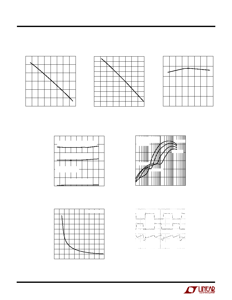
TYPICAL PERFOR A CE CHARACTERISTICS
U
W
Undervoltage Lockout Trip
Voltage (Falling) vs Temperature
TEMPERATURE (
°
C)
60
1.85
INPUT VOLTAGE (V)
1.90
1.95
2.00
2.05
20
20
60
100
3701 G04
2.10
2.15
40
0
40
80
Undervoltage Lockout Trip
Voltage (Rising) vs Temperature
TEMPERATURE (
°
C)
60
2.00
INPUT VOLTAGE (V)
2.02
2.06
2.08
2.10
2.20
2.14
20
20
40
3701 G05
2.04
2.16
2.18
2.12
40
0
60
80
100
Maximum Current Sense
Threshold vs Temperature
Input and Shutdown Currents vs
Input Voltage
Efficiency vs Load Current (Pulse
Skipping Mode)
PGOOD R
ON
vs Input Voltage
2-Phase Operation
TEMPERATURE (
°
C)
60
MAXIMUM CURRENT SENSE THRESHOLD (mV)
125
120
115
110
105
100
0
40
100
3701 G06
40 20
20
60
80
INPUT VOLTAGE (V)
2
INPUT CURRENT (
µ
A)
4
6
7
11
3701 G07
3
5
8
9
10
600
500
400
300
200
100
0
PULSE SKIPPING MODE OPERATION
(EXTCLK/MODE = 0V)
BURST MODE OPERATION
(EXTCLK/MODE = V
IN
)
SHUTDOWN
(I
TH
/RUN
1,2
= 0V)
FIGURE 1 CIRCUIT
LOAD CURRENT = 0A
LOAD CURRENT (mA)
EFFICIENCY (%)
100
90
80
70
60
50
40
1
100
100O
1OOOO
3701 G08
10
FIGURE 1 CIRCUIT
EXTCLK/MODE = GND
V
OUT
= 2.5V
V
IN
= 3.3V
V
IN
= 4.2V
V
IN
= 6V
V
IN
= 8.4V
INPUT VOLTAGE (V)
500
450
400
350
300
250
200
150
100
50
0
PGOOD R
DS(ON)
(
)
3701 G09
0
1
2
3
4
5
6
7
8
9
10
I
PGOOD
= 500
µ
A
SW1
5V/DIV
SW2
5V/DIV
INPUT
CURRENT
1A/DIV
FIGURE 1 CIRCUIT
500ns/DIV

5
LTC3701
3701fa
U
U
U
PI FU CTIO S
SENSE1
, SENSE2
(Pins 1, 8): The () Inputs to the
Differential Current Comparators.
I
TH
/RUN1, I
TH
/RUN2 (Pins 2, 6): These pins each serve
two functions. Each pin serves as the error amplifier
compensation point as well as the run control input for the
respective controller. Forcing one pin below 0.35V causes
the functions associated with that controller to be shut
down. Forcing both I
TH/RUN
pins below 0.35V causes the
device to be shut down. Nominal operating voltage range
on these pins is from 0.7V to 1.9V.
V
FB1
, V
FB2
(Pins 3, 5): Each receives the remotely sensed
feedback voltage for each controller from an external
resistive divider across the output.
SGND (Pin 4): Signal Ground.
PLLLPF (Pin 7): Serves as the lowpass filter point for the
PLL and as the voltage control input to the internal
oscillator. Normally, a series RC is connected between this
pin and ground when synchronizing to an external clock.
Nominal voltage range is from 0V to 2.4V. Frequency can
be set by forcing this pin with a voltage. Tying this pin to
GND selects 300kHz. Tying to V
IN
or a voltage
2.4V
selects 750kHz. Floating this pin selects 550kHz opera-
tion.
SENSE2
+
(PV
IN2
), SENSE1
+
(PV
IN1
) (Pins 9, 16): The (+)
Inputs to the Differential Current Comparators. These pins
also power the gate drivers.
EXTCLK/MODE (Pin 10): External Clock Input. Applying a
clock to this pin causes the internal oscillator to phase-
lock to the external clock (nominal lock frequency range
between 300kHz and 750kHz). This also disables Burst
Mode
operation but allows pulse-skipping at low load
currents.
Forcing this pin high enables Burst Mode operation.
Forcing this pin low enables pulse-skipping mode. In
these cases, the frequency of the internal oscillator is set
by the voltage on the PLLLPF pin. If the PLLLPF voltage is
not set externally, the frequency internally defaults to
550kHz.
PGOOD (Pin 11): Power Good Output Voltage Monitor
Open-Drain Logic Output. This pin is pulled to ground
when the voltage on either feedback pin (V
FB1
, V
FB2
) is not
within
±
8% of its nominal set point. PGOOD is pulled low
when channel 1 or both channels are shut down. When
channel 2 is shut down and channel 1 enabled, the
PGOOD output indicates the state of V
FB1
only.
PGATE2, PGATE1 (Pins 12, 14): Gate Drivers for the
External P-Channel MOSFETs. These pins swing from 0 to
SENSE
+
(PV
IN
).
PGND (Pin 13): Ground Pin for Gate Drivers.
V
IN
(Pin 15): Chip Signal Power Supply Input. This pin
powers the entire chip except for the gate drivers.